
P - N Junction


What is a P-N Junction?

A P-N Junction is a boundary between p-type semiconductors and n-type semiconductors built inside a single crystal semiconductor.

Most of the electronic appliances such as diodes, transistors and integrated circuits (IC s) work on the action of the P-N junction.
It is impossible to make a P-N junction just by joining a P-type semiconductor and a N-type semiconductor.

A sample P-N junction will be as follows:


The right half of the above junction has been doped with an element in the 15th group of the periodic table so that it makes a n type semiconductor. For example As (Arsenic) can be used to dope these n type semiconductors. The donor cations shown in the above diagram represent As+ ions.

In contrast, the left half of the above junction has been doped with an element in the 13th period of the periodic table so that it makes a p type semiconductor. For example B (Boron) can be used to dope these p type semiconductors. The receiver anions shown in the above diagram represent B- ions.


(Photo credit : pveducation.org)

Both these anions and the cations are firmly bonded to the crystal lattice structure.

The small circles in the left side represent the holes created by the receiver atoms.

For simplicity let us ignore the atoms belonging to the semiconductor in the above diagram.

The boundary where the p - type semiconductor (or the left side in the above figure) and the n-type semiconductor (or the right side in the above figure) meet is called the p-n junction.

When such a p-n junction is made different carriers inside the p-n semiconductor move in arbitrary directions. However, the concentration of holes in the p region is greater than that in the n region. Furthermore, when two holes approach each other mutual repulsion occurs.


(Photo credit: electrapk.com)


Due to these two reasons, holes close to the junction diffuse from the p side to the n side. For a similar reason, electrons close to the junction diffuse from the n side to the p side.


(Photo credit: haribrahma.wordpress.com)

Furthermore due to the mutual attraction between the holes and the electrons, both these carriers will not further remain as 'free electrons'.

Thus, at some instant after initiating these movements the region close to the junction becomes void of 'free carriers'.


(Photo credit : electronics.stackexchange.com)

Meanwhile due to this diffusion process, the p part close the junction, which was then a neutral region, now becomes a negatively charged region and the n part close to the junction becomes a positively charged region.

These two newly formed layers of positive and negative charges are similar to a parallel plate capacitor.


(Photo credit: Boundless.com)

Thus a potential difference and an electric field is formed in this region.

However the direction of the electric field is such that it is against the diffusion of the major carriers.


Although the magnitude of the electric field increases as soon as the junction was created, when the diffusion of the carriers decreases, its magnitude decreases and gains a state of equilibrium.

Since, after gaining equilibrium, a small area close to the junction is void of carriers, this region where there is a large resistance layer. Its thickness is about 1 μm.


(Photo credit: topperchoice.com)

The potential difference that is created in this layer depends upon the nature of the p-n junction. For example, the potential difference for silicon is about 0.7 V and that for Germanium is about 0.3 V.

This is known as the potential barrier over the p-n junction.

All these data can be summarized in a graph as follows:


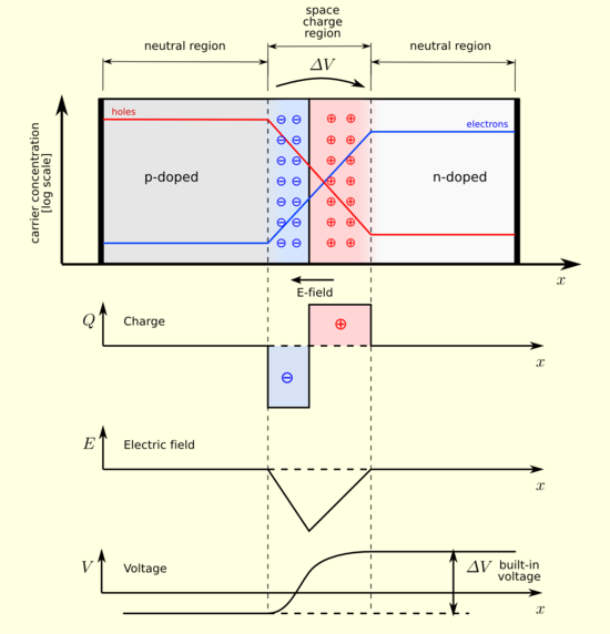
(Photo credit: Wikipedia)

Comments

Popular posts from this blog

Action of a transistor

In this note I will present details only about the npn transistor. For those who are interested only on the pnp transistor, you can switch the action of the npn transistor and the behavior of current to adjust with the characteristics of the pnp transistor. (Photo credit: mahasona10000.blogspot.com ) As in the case of a p-n junction,the two n parts of the npn transistor contain an excess of free electrons. In contrast, the p part contains excess holes. As in the case of the p-n junction, in the npn transistor depletion regions develop and junction barriers occur. (Photo credit: daenotes.com) For the correct functioning of the transistor, the first p-n junction is forward biased and the second p-n junction is reverse biased. This results for the first p-n junction to be of low resistance and the second p-n junction to be of high resistance. (Photo credit: www.nzart.org.nz ) The letters of these elements

Gold leaf electroscope

What is a gold leaf electroscope? Gold leaf electroscope is an instrument for detecting and measuring static electricity or voltage. The following diagram shows a modern gold leaf electroscope: Why is gold used to make such an electroscope? Gold is popularly used to make such electroscopes since gold is even sensitive to very minute charges (This is achieved by the malleability of gold - hammering into sheet form and making the mass thin). When we introduce a charged object to the disk of the electroscope ( explained below) we practically do not know the magnitude of the charge. Thus a simple conductor may not be the best option to show a reasonable deflection or response even to minute charges. Thus gold is assumed to be sensitive to charges of any magnitude which makes it more suitable as the indicator.  Besides gold is also a non corrosive metal. We practically do not use anhydrous materials inside the glass case. The penetration of

The Silver Mirror Test

What is the Silver Mirror Test? Silver Mirror Test is a test that is used to differentiate between aldose and ketose sugars using the Tollen's reagent. Tollen's reagent is an alkaline solution of ammoniacal silver nitrate and is used to test for aldehydes. *Ketones do not react with the Tollen's reagent. Silver ions in the presence of hydroxide ions form a brown precipitate of silver (I) oxide, Ag 2 O (s) . Ag 2 O This precipitate dissolves in aqueous ammonia, forming the diamminesilver(I) ion, [Ag(NH 3 ) 2 ] + . The reactions that take place in this experiment are as follows: 2Ag + (aq)  + 2OH - (aq)   →   Ag 2 O (s)  + H 2 O (l) Ag 2 O (s)  + 4NH 3 (aq)  + H 2 O (l)   →  2[Ag(NH 3 ) 2 ] + (aq)  + 2OH - (aq) What happens if Silver Nitrate is used without ammonia or why is ammonia used in this experiment? When ammonia is added to the silver nitrate solution, silver ions are less prone to reduction. Thus, silver is produce

Electromagnetic Induction

What is electromagnetic induction? When an alternative current is allowed to flow through a certain circuit and that circuit is kept near a neutral circuit, the former circuit induces charge distributions in the latter circuit resulting in an induced current in the latter circuit. This phenomenon is called the electromagnetic induction. Thus a potential difference arises across the circuit when exposed to a varying magnetic field. Faraday's law- Any change in the magnetic environment of a coil of wire will cause a voltage (emf) to be "induced" in the coil.  (Photo credit: gic-edu.com) Thus, fluctuating magnetic fields cause currents to flow in conductors placed within them. This is called induction because there is no physical connection between the conductor and the magnet. The current is said to be induced in the conductor by the magnetic field. In order to produce the maximum force needed for induction, usually the cond

Flame test- By Aditya Abeysinghe

Introduction: Flame test is an experiment used to identify/distinguish metals using colors exposed to a flame.  Since metallic halides easily evaporate, the test is usually done using the halide components of metals. Out of the halides, chlorides are frequently used because chlorides give a fast change of color when exposed to the flame as opposed to other halides. Materials needed:       ·           A rod of platinum, nichrome, asbestos or graphite      ·          Concentrated HCl solution      ·          Bunsen burner      ·          Metallic salt (a chloride of a metal)      ·          A cobalt glass (if necessary) Method: Insert the rod of platinum, nichrome, asbestos or graphite into a concentrated solution of HCl. Hold the rod to a Bunsen flame. (to the  colorless region) Continue this experiment until the top region of the flame turns colorless. Form a pulp by mixing the metallic salt with the concentrated HCl solution and apply